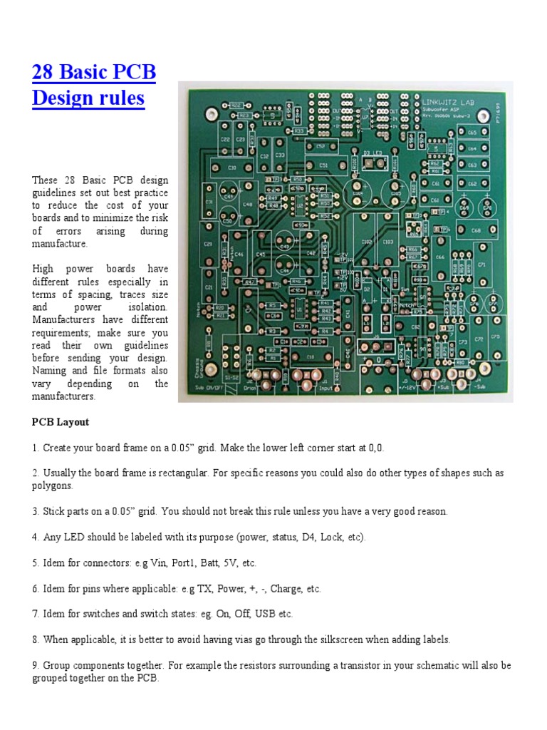
Pcb Train Design Rules
As indicated in the design flow, the set/check cbd (correct by design) rules and constraints step will now be discussed. Each box in this flow represents a common step in the design of a printed circuit board.

Ddr4 Pcb Design PCB Circuits
While there are some free pcb design software programs, most of these programs require a fee to use.

Pcb train design rules. Any text placed in a copper layer has to comply with the design rules for the given class (see classification table). Meta dpcb train supply production & prototype pcb services. To sum up, high speed pcb design is applied to devices with pcbs working at high frequencies with the use of high speed interfaces.
When you begin to design your rigid flex pcb, there are a few rules you want to adhere to as best as possible: General layout guidelines for printed circuit boards (pcb), which exist in relatively obscure documents, are summarized. When making a bend, keep the bend curved rather than sharp.
Design rule checking or check (s) (drc) is the area of electronic design automation that determines whether the physical layout of a particular chip layout satisfies a series of recommended parameters called design rules. Design rule checking is a major step during physical verification signoff on the design, which also involves lvs (layout versus. The design of the printed circuit board can be as important as the circuit design to the overall performance of the final system.
When i was growing up, my parents had a cuckoo clock on the wall of our dining room. For pcbs ≥ 0,8mm thickness 0,75% with smd 1,50% without smd please note that the twist & bow value is increased above average, if the copper balance of the pcb is locally very unequal or if the circuit board is very thin. The orthogonal routing rule states that.
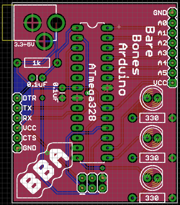
The common pcb layout rules of thumb. Use pcb train for less demanding components pull up resistors, decoupling capacitors and any other component in a design that really doesn't require the highest specification, should all be picked from our pcb train stock. 1 • most important step in designing a pcb • intelligent placement makes routing easy • typically can place circuit in "blocks" • keep components close together (shorter traces typically are better) • keep power dissipation in mind (spacing/trace widths) •.
It was old, it was made of wood and other magical parts, and the little bird popped out and. For some designers, the pcb design will be a natural and easy extension of the design process. Fortunately, there are a couple of simple rules that can mitigate this commercial risk, and both have their root in the design function.
Gradually change the width of the traces. Printed circuit boards (pcbs) are created by layering insulating material and electrical conductors. The design tools that you will need for laying out analog circuitry.
• creates microstrips (see figure) for traces running over it (controls impedance) • minimizes radiating and pickup loop area. All copper text must be correctly readable. A clock composited on a printed circuit board.
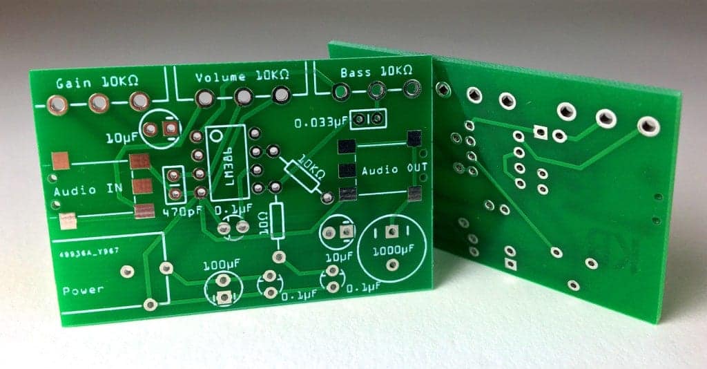
Get a quote online today.escription 1 Pcb technical advice for pcb design and fabrication tips Five pcb design guidelines for analog circuits.
Freepcb freepcb is an open. Printed circuit boards that work on relatively higher power have an entirely different set of design guidelines when it comes to issues such as power isolation, track widths, track. The size of the printed circuit board is very small, and the location of the components becomes a real challenge (especially when you come across a high speed interface layout).
The circuit boards are either single or multiple sided. We shall discuss in this chapter the partitioning of the circuitry, the problem of interconnecting traces, parasitic components, grounding schemes, and. Circuit design rules wiring is the most important process in the entire pcb design.
In order to reduce the chances of manufacturing errors and to lower the cost of your printed circuit boards, the following pcb design guidelines are set for best practice. Without further adieu, let's break down some common pcb layout rules of thumb and see if we can provide some helpful context behind these design rules. Pcb design tutorial by david l.
This will directly affect the performance of the pcb board. Abruptly changing the trace width could result in a. Try not to bend at the corners.
As a uk pcb supplier we are able to turn around orders within 24 hours. Pcb design tools allow designers to create the layouts for these boards. I discussed this particular rule of thumb in a recent article, so i'll only repeat the important points here.
Some guidelines apply specifically to microcontrollers; Jones page 3 of 25 3 introduction you've designed your circuit, perhaps even bread boarded a working prototype, and now it's time to turn it into a nice printed circuit board (pcb) design. However, the guidelines are intended to be general, and apply to virtually a ll modern cmos integrated circuits.
Therefore, whether you are a pcb design beginner or a pcb design practitioner, the basic design rules of pcb are design skills that everyone must master, including pcb design theory and board rules.

Esd Pcb Design Guidelines PCB Circuits
Basic PCB Design Rules Printed Circuit Board
Eagle Pcb Design Rules Pdf PCB Designs
PCB Design Rules Royal Circuit Solutions

PCB Layout Fast Forward DDR3 Memory Layout YouTube
How to Design a PCB Layout Circuit Basics
How to Design PCB Layout Rules That Work


Design Rules for rigidflex board Hitech Circuits Co., Ltd.

pcb design Help check my pcb layout and routing please

17. PCB design part IV design rules check YouTube
Some LVDS PCB Layout Guidelines for Ensuring Signal

Realistic design rules for a homemade PCB Layout KiCad

PCB Offerings Board level Components, Layout and Design

Basic PCB design rules that you must follow to make error

PCB Engineering Solutions Venture Elctronics

Why impose PCB design constraints? Part 2 « PADS Desktop
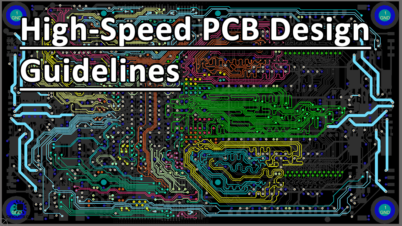
HighSpeed PCB Design Guidelines

Basic rules of the PCB design. Download Scientific Diagram
schematics PCB layout rules Electrical Engineering